We are very excited to be going to Portland OR for ISTFA 2019. This is always a great show and we are looking forward to meeting with friends and making new ones. Please visit us at Booth #306.
We will be at there representing a number of products:
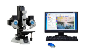
Micro Support Micromanipulators
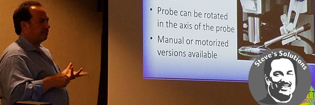
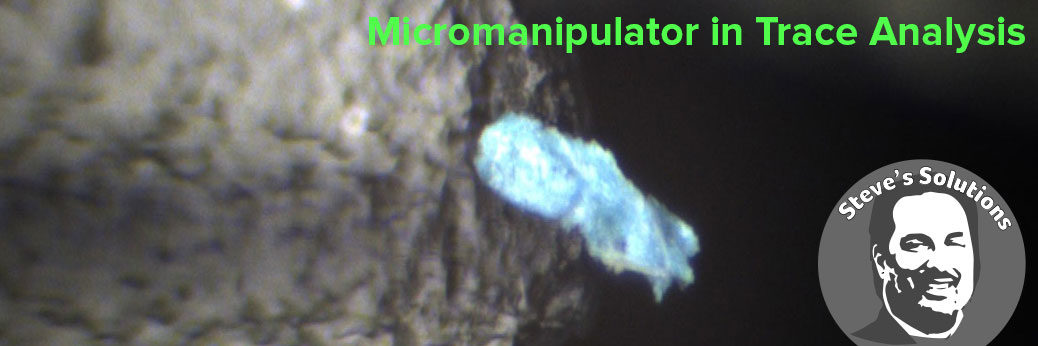
Microscope/micromanipulator system to easily perform sample manipulations as small as 1 micron. Probes available for a wide range of sample manipulations, including:
Electrical Probing
Isolating particles
Cutting
Milling off a surface
Micro tweezers
Vacuum for particle transfer
Arms also be added to FTIR or Raman Microscopes
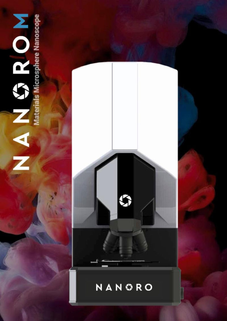
Nanoro
The Nanoro M is a cutting edge light microscope which can break the optical diffraction limit using the Super-Resolution Microsphere Amplifying Lens (SMAL).
About ISFA 2019, October 2-3, Phoenix Convention Center
Plan today to attend ISTFA 2019! The 44rd International Symposium for Testing and Failure Analysis (ISTFA). This year’s theme is ‘ Failures Worth Analyzing’
We will be demonstrating the Microsupport Axis Pro micromanipulator at the Golden Gate Polymer Forum Two-Day Short Course: Polymers in Electronic Packaging on November 4-5, 2019
This two-day day short course, presented by recognized experts from The Madison Group, is based on their annual course “Plastic Part Failure: Analysis, Design and Prevention” given at the University of Wisconsin – Milwaukee. Attendees will gain a better understanding of basic principles that affect the durability and failure of plastic parts. As these speakers like to say “if you don’t know how something broke, you can’t fix it,” highlighting the importance of a thorough understanding of how and why a product has failed. With emphasis on practical problem-solving techniques, the course will utilize case studies to comprehend key aspects of plastic failure and prevention. Gain a better understanding of why plastic components fail, and how to avoid future failures by applying the knowledge learned. The combination of excellent speakers, a convenient location in the Bay Area, an affordable price, and focus on practical applications makes this an exceptional opportunity.
Cathodoluminescence offers a quick, non-invasive approach to determining alloy compositions, exposing defects and uncovering surface contamination
All compound semiconductor chipmakers, from the producers of LEDs, lasers and solar cells to the makers of power and RF devices, need to characterize their material. It is an essential step in the production process that can expose and identify any imperfections in epiwafers, and may save money and reputation, by avoiding the production of devices with dubious characteristics.
Cathodoluminescence is one of the many techniques that may be used to characterise epiwafers. It involves directing a beam of electrons at the surface of a wafer, and collecting, in parallel, secondary electrons and an optical signature. Data extracted from these distinct signals are complementary and offer much insight into the characteristics of the material. For example, imaging cathodoluminescence intensity highlights both buried and surface defects, and the latter can be distinguished from the former using a secondary electron image taken in parallel (see Figure 1).
Figure 1. The Attolight Säntis 300 can provide scanning electron (SE) and panchromatic cathodoluminescence (CL) images. Shown here are 7 µm by 7 µm images of a microLED. The largest dark spot is attributed to a speck of dust, visible in the scanning electron image. Several types of buried defects can be identified in the cathodoluminescence map.
At Attolight of Lausanne, Switzerland, engineers have developed a portfolio of cathodoluminescence instruments, including Säntis 300, an instrument capable of full-wafer mapping (for details of this tool, and its capabilities, see Capabilities and strengths of Säntis 300). Read on to discover how this tool has been used by GaAs solar cell producer Alta Devices to undertake three particular tasks: to speed and trim the costs associated with developing the process for producing AlGaAs layers with well-defined compositions; to detect defects detrimental to device performance; and to expose surface contamination. Note, moreover, that Alta Devices also use cathodoluminescence for new layer design development.
Characterising composition
To optimise the performance of GaAs solar cells, makers of these devices must produce homogeneous layers of AlGaAs alloys with a composition that is very close to the target value. Success in this endeavour often involves measuring the composition of AlGaAs epilayers with Auger electron spectroscopy, but cathodoluminescence offers a superior alternative.
One of the merits, benefitting the engineers at Alta Devices, is the substantial cost saving associated with preparing a reactor for its initial production of solar cells. Prior to the growth of this photovoltaic structure, calibration runs are required, with typically five cycles needed to tune homogeneity, and a further five to tune the ratio of aluminium to gallium in the AlGaAs epilayers.
Savings of around $50,000 are realised by carrying out this initial tuning with cathodoluminescence, rather than the more common approach, Auger electron spectroscopy. The reduced expenditure partly stems from making the measurement in-house, rather than shipping a sample to a specialist that will take several days to provide a result. In addition, as Auger electron spectroscopy is a destructive technique, a cost comes from being unable to re-use the base wafer.
Figure 2. (top) Cross-sectional scanning-electron imaging of a multilayer AlxGa1-xAs stack together with a diagram of the structure. The sample is used for the initial cathodoluminescence calibration with respect to Auger electron spectroscopy. (bottom left) cathodoluminescence spectra extracted from material A and B, exhibiting distinct spectral features. (c) application of the obtained calibration in top view, production mode, to obtain a composition for material B.
Another advantage that cathodoluminescence has over Auger electron spectroscopy is that it offers greater insight into the characteristics of the wafer. Whether undertaking initial tuning, quality control or R&D, cathodoluminescence provides a faster turnaround and better statistics. Operating in an automated step and repeat mode, this technique can determine alloy composition at more than 120 points per wafer in less than 5 minutes. In comparison, it takes an hour to measure one point on a wafer by Auger electron spectroscopy.
Cathodoluminescence is also a very powerful tool in a production environment. As it is non-contact, there is no need to scrap any base material. Instead, samples can be returned to the production batch after they have been inspected. Higher production yields are also possible – measurements typically take much less than 30 minutes, so if there is a problem with the growth process, this should become apparent before a second out-of-specification run begins.
Identifying sub-surface defects…
When producing GaAs solar cells – or, for that matter, power and RF electronic devices – a major concern is the class of defect that can cause a short circuit between the active layers. This type of defect is hard to spot, as it is not visible by either scanning electron microscopy, optical microscopy or atomic force microscopy.
Figure 3. (left) Identifying defects with cathodoluminescence, rather than the electron beam induced current technique, trimmed the turnaround time for defect density determination and process adjustments by a factor of ten. (top right) cathodoluminescence imaging, centred on the GaAs band edge emission, exposes crystalline defects. Comparing points 1 and 2 with spectral scans (see bottom right), shows that only the GaAs peak suffers a variation. This suggests that the defect spotted at point 2 is actually in the GaAs layer of the stack, not in the other layer emitting the light in the peak to the left of it.
Prior to the availability of cathodoluminescence, defects were identified by an electron beam induced current. However, this measurement has to be carried out on the final device, resulting in a time delay before the process can be adjusted. With cathodoluminescence, this time is divided by ten, because the very same defects can be identified right after the epi process. This significantly speeds the development process and produces material with better properties – and ultimately a better average device quality. The non-contact, non-destructive nature of cathodoluminescence also pays dividends. If the material is good, production steps can proceed on analysed samples.
Obviously, a non-destructive technique doesn’t save money when epiwafers are poor, and need to be scrapped. However, the speed of this technique enables a saving associated with avoiding unnecessary processing on sub-standard wafers.
Yet another merit of cathodoluminescence is the greater insight it offers, compared with the electron beam induced current technique. This aids root cause identification, because with cathodoluminescence, the layer containing the crystalline defect can be identified by its detailed spectral signature.
… and surface contamination
When surface contaminants are on the epiwafers, they tend to have a significant impact on surface luminescence and absorption. Consequently, there is an opportunity to quantify their relative density by cathodoluminescence. This is particularly useful with photonic materials, as contaminants can drag down device efficiency.
The strengths of cathodoluminescence – it is able to expose surface contaminants, uncover defects that can cause a short circuit, and provide a quick, insightful approach to determining alloy compositions – are sure to spur interest in this tool. However, like all inspection instruments, how much value it offers will be debated by potential customers, who will try to consider its capability with new process technologies.
Intuitively, inspection and metrology tools have always been put into the ‘non-value-added’ bin. That’s never the case with process tools, as they can modify production steps, making devices cheaper, better, or possible both. Over the past few decades this stance is softening, with the ratio of investment in metrology tools to process tools climbing from around 2 percent to 10 percent, according to VLSI Research. This is a testament to the critical impact provided by the right inspection and metrology tools.
For the compound semiconductor chipmakers, there is tremendous value in managing point and line defects and measuring and controlling the composition of alloys. The merits of this, highlighted by the efforts of GaAs solar cell maker Alta Devices and detailed in this article, champion the virtues of cathodoluminescence. They are not limited to measuring GaAs solar cells, but extend to GaAs photonics and all compound semiconductor devices, and can be summed up as three key strengths. They are: a faster turnaround in R&D and process development, speeding the time to market for new technologies; a non-invasive nature, which enables more frequent process control with no impact on production, while avoiding scrapping analysed samples and slashing the cost of metrology; and improved process metrology statistics, enabling tighter process control and directly impacting production quality, so a greater proportion of devices go into top-selling bins. All these assets make a meaningful impact by improving a fab’s balance sheet.
BY CHRISTIAN MONACHON AND SYLVAIN MUCKENHIRN FROM ATTOLIGHT AND HASTI MAJIDI AND CHRIS FRANCE FROM ALTA DEVICES
We are very excited to be attending SciX 2019 in beautiful Palm Springs California.
Come visit us at booth #514 where we will be showing the Micro Manipulators from MicroSupport.
Micro Support Micromanipulators
Microscope/micromanipulator system to easily perform sample manipulations as small as 1 micron. Probes available for a wide range of sample manipulations, including:
Isolating particles
Cutting
Milling off a surface
Micro tweezers
Vacuum for particle transfer
Arms also be added to FTIR or Raman Microscopes
OSTEC
Ostec Corporate Group produces and offers hi-tech innovative scientific and analytical equipment.
SciX 2019, October 13-18, 2019 in Palm Springs, California
Leading researchers will convene to present their cutting edge developments in analytical sciences, instrumentation, and unique applications. The SciX meeting hosts a world-class exhibition, presentations from leading scientists, educational courses, and many networking opportunities.
Geophysical Laboratory’s Zachary Geballe Receives Seventh Postdoctoral innovation and Excellence Award
The Geophysical Laboratory’s Postdoctoral Associate Zachary Geballe has been honored with Carnegie’s seventh Postdoctoral Innovation and Excellence (PIE) Award. These prizes are made through nominations from the departments and are chosen by the Office of the President. Geballe, in Viktor Struzhkin’s lab, was awarded the prize for his scientific innovations and community service to the Broad Branch Road (BBR) campus.
Zack works on developing methods to measure the heat capacities of metals and silicates at high pressures. This work applies to developing new materials and studying the deep interiors of planets. He developed a pioneering technique to measure heat in a diamond anvil cell (DAC) by using a method called the alternating current 3rd harmonic method. The work was published in two recent papers in the Journal of Applied Physics. Additionally, he devised new, sophisticated sample loading procedures into the DAC with micro-manipulator equipment. The new approach has changed the way the group loads very small samples for high-pressure experiments.
The nomination stated that “Zack is much more than just a very skillful and dedicated experimentalist, he is also the leader of our weekly Bread and Cheese seminar with research updates from our own scientists and discussions of high-impact papers from other groups around the world. “
Additionally, Zack was a founding organizer of postdoc-led poster sessions at the BBR campus (see photos and details from 2015, 2016, and 2017), which have featured the work of nearly all the researchers and sparked new collaborations, approaches, and teamwork.
Carnegie President Matthew Scott remarked, “This cycle of nominations was particularly strong and it was a difficult choice. Zack’s exceptionally creative approaches to scientific innovation and his extraordinary volunteer efforts have made a significant contribution to the sense of community at BBR, making him the high caliber of researcher and colleague envisioned for the PIE awards to recognize. I congratulate him on his accomplishments.”
We are very excited to be attending Microscopy & Microanalysis 2019 meeting in Portland OR, August 4-8, 2019. Come visit us at booth #1030.
We will be higlighting our MicroSupport Micromanipulator system.
MicroSupport
Micro Support Micromanipulators
Manipulation of small materials.Probes available for a wide range of sample manipulations, including:
Isolating particles
Cutting
Milling off a surface
Nanoliquid deposition
Vacuum for material removal
Arms also be added to FTIR or Raman Microscopes.
Attolight
Attolight manufactures the leading cathodoluminescence (CL) microscopes and accessories on the market. These systems have been used for a range of applications, including:
Defect Visualization and Counting in Optoelectronic Materials
GaN for Power Electronics
Photovoltaic Materials
Defects in Thin Film Battery Materials
Semiconducting Diamond
About Microscopy & Microanalysis
The largest microscopy/microanalysis instrument exhibition in the world. Plan to visit the more than 100 companies displaying their latest technology and services. The social activities of the opening reception, and daily “happy hours” accompanying each day’s poster and awards sessions, have become “can’t-miss” events of learning and fellowship
We are very excited to be attending SemiCon west 2019 in San Francisco, CA July 9-11. We will be showing the following technologies.
Micro Support Micromanipulators
Manipulation of small materials.Probes available for a wide range of sample manipulations, including:
Isolating particles
Cutting
Milling off a surface
Nanoliquid deposition
Vacuum for material removal
Arms also be added to FTIR or Raman Microscopes.
Attolight
Attolight manufactures the leading cathodoluminescence (CL) microscopes and accessories on the market. These systems have been used for a range of applications, including:
Defect Visualization and Counting in Optoelectronic Materials
GaN for Power Electronics
Photovoltaic Materials
Defects in Thin Film Battery Materials
Semiconducting Diamond
About SEMICON West
Three days of presentations with more than 80+ hours of technical and business programming, plus hundreds of exhibitors provide the insights, innovations, and intelligence you need to get ahead and embrace today’s disruptive landscape.
From materials, equipment, design, manufacturing, system integration, and demand channels to new verticals and adjacencies such as Flexible Hybrid Electronics, MEMS & Sensors, you’ll gain access to the best in the business and get a glimpse at what’s next. Immersive, new experiences demonstrating hot-buttons like Smart Transportation, Smart Manufacturing, MedTech, Big Data, IoT, and the cognitive technologies that are transforming the world make this year’s Expo like no other before.
We are very excited to be attending the American Institute for Conservation and the Foundation for Advancement in Conservation Annual Meeting MAY 13-17, 2019 Uncasville, CT
We will be at booth #106 representing a number of products:
Micro Support Micromanipulators
Manipulation of small materials.Probes available for a wide range of sample manipulations, including:
The International Day of Light is a global initiative highlighting to the the citizens of the world the importance of light and light-based technologies in their lives, for their futures, and for the development of Society.
Barnett-Technical Services supports the International Day of Light and its annual celebration on May 16th.
We are very excited to be attending the Southern Association of Forensic Scientists joint meeting with the American Association of Trace Evidence Examiners May 1 – 3, 2019 in Asheville, NC.
We will be featuring our Micro Support Micromanipulator.
Micro Support Micromanipulators
Manipulation of small materials. Probes available for a wide range of sample manipulations, including: