We are happy to announce that Barnett Technical Services is now a distributor for Hot Disk® instruments in the Western United States and Canada. These instruments provide fast, easy and non-destructive measurement of thermal conductivity, thermal diffusivity and specific heat capacity. Click here for more information
All posts by 27481873
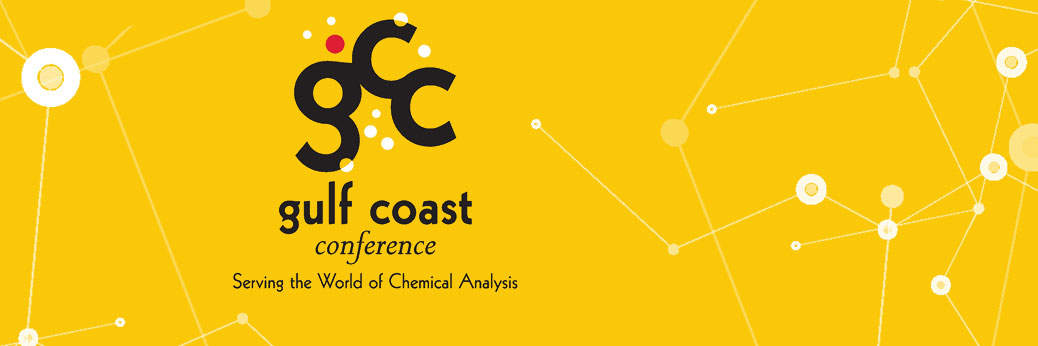
Gulf Coast Conference 2023
We are very excited to be attending GCC 2023 in Galveston Texas. Please visit us in Booth #315.
We will be showing the Micro Manipulators from MicroSupport.
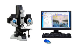
Micro Support Micromanipulators
Microscope/micromanipulator system to easily perform sample manipulations as small as 1 micron. Probes available for a wide range of sample manipulations, including:
- Isolating particles
- Cutting
- Milling off a surface
- Micro tweezers
- Vacuum for particle transfer
Arms also be added to FTIR or Raman Microscopes
Gulf Coast Conference, October 11-12, 2023 in Galveston, Texas
The Gulf Coast Conference is a non-profit organization oriented toward the education and advancement of knowledge of Chemical Analysis Technology associated with the Petrochemical, Refining, and Environmental fields, and will forward this goal through annual technical meetings, regular communications, and training courses focused on these fields.
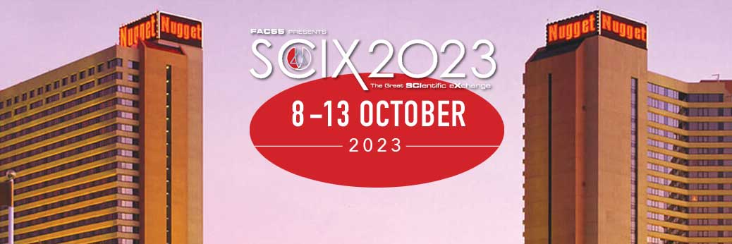
SciX 2023
We are very excited to be attending SciX 2023 in Sparks, NV.
Come visit us at booth #316 where we will be showing the Micro Manipulators from Micro Support.
Micro Support Micromanipulators
Microscope/micromanipulator system to easily perform sample manipulations as small as 1 micron. Probes available for a wide range of sample manipulations, including:
- Isolating particles
- Cutting
- Milling off a surface
- Micro tweezers
- Vacuum for particle transfer
Arms also be added to FTIR or Raman Microscopes
SciX 2023 conference October 8-13, 2022 in Sparks, Nevada
Leading researchers will convene to present their cutting edge developments in analytical sciences, instrumentation, and unique applications. The SciX meeting hosts a world-class exhibition, presentations from leading scientists, educational courses, and many networking opportunities.
This is a special year as it will be the 50th annual FACSS conference! With special sessions and special guests to honor this milestone, this is a year you won’t want to miss!
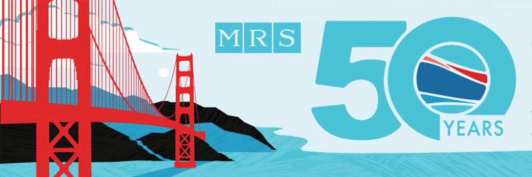
MRS Spring 2023
We are very excited to be attending Materials Research Society Spring Meeting, April 10-14, 2023, in San Francisco, California. We will be at booth #219 representing a number of products:
Micro Support Micromanipulators
Manipulation of small materials. Probes available for a wide range of sample manipulations, including Isolating particles, Cutting, Milling off a surface, Nanoliquid deposition, Vacuum for material removal. Arms also be added to FTIR or Raman Microscopes.
SOL Raman
Manufacturers of advanced Raman microscopes including rapid Raman imaging and CARS microscopy systems.
Lasertec
Manufacturers of laser confocal microscopes.
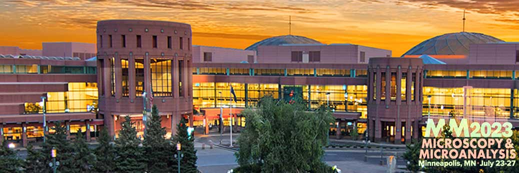
Microscopy & Microanalysis 2023
We are very excited to be attending Microscopy & Microanalysis 2023 meeting in Minneapolis MN, July 23 – 27, 2023. Come visit us at booth #1038
Hands on Micromanipulator Tutorials
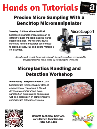
BTS will be giving two workshops on our Micro Support micromanipulator – one on basic micromanipulator use and a second on microplastics handling and detection. Sign up at our booth!
Precise Micro Sampling With a Benchtop Micromanipulator Tutorial
Tuesday 7/25/2023 – 5:45 pm at booth #1038
Microscopic sample preparation can be difficult to near impossible as structures become smaller. We will show how a benchtop micromanipulator can be used to probe, scrape, cut, and isolate materials on a surface. The system can also be configured to allow these microsampling operations inside a glovebox.
Attendees will be able to work directly with the system and are encouraged to bring samples they would like to try out during the Workshop.
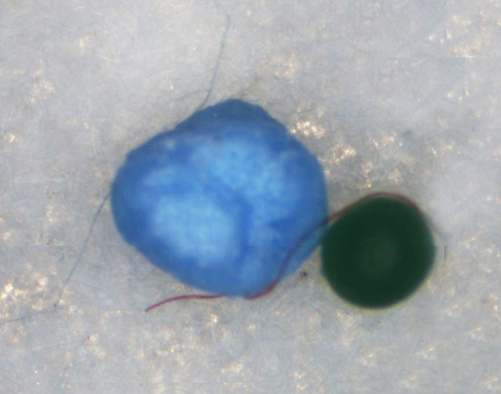
Microplastics Handling and Detection Workshop
Wednesday 7/26/2023- 5:45 pm at booth #1038
Microplastics represent a new class of environmental contaminant that has been increasing over time throughout the world. We will demonstrate imaging and micro sampling using the Micro Support Axis Pro micromanipulator on microplastics samples. We will also speak about Soar Optics class of comprehensive microplastics detection systems and where we see the future of microplastics detection.
Come Speak to us about these products:
Micro Support Micromanipulators
These cutting-edge tools specialize in the precise manipulation of miniature materials. Equipped with an array of versatile probes, they offer a broad range of capabilities for handling various samples. Key features include:
- Particle Isolation: Effortlessly isolate particles with exceptional accuracy.
- Cutting: Seamlessly perform precise cuts on minute objects.
- Surface Milling: Remove layers from surfaces with utmost precision.
- Nano liquid Deposition: Achieve meticulous placement of nano liquids for intricate applications.
- Vacuum-Assisted Material Removal: Utilize vacuum functionality to efficiently remove unwanted materials.
Moreover, these micromanipulators can be seamlessly integrated with FTIR or Raman microscopes, enhancing their functionality by incorporating additional arms.
Experience unparalleled control and dexterity in manipulating small-scale materials with the Micro Support micromanipulators.
Click here to learn more about the Axis Pro Micromanipulator.
Lasertec Confocal Laser Scanning Microscopes
The industry’s first hybrid laser microscope that utilizes the benefits of white light and laser confocal microscopy. The HYBRID + brings multiple cutting edge technologies together into one package.
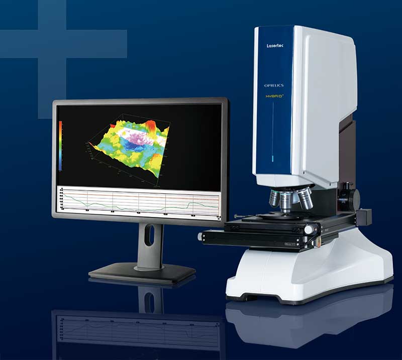
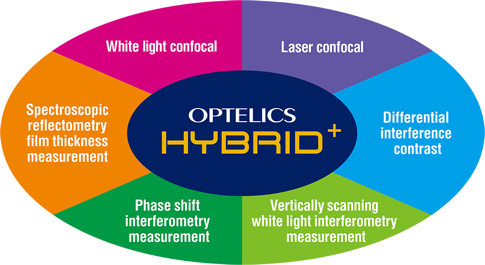
Click here to learn more about Lasertec instruments
SOL Raman Microscopes
SOL Instruments offers a wide range of Raman microscopes from simple microscopy solutions to advanced Raman microscopes and commercial CARS systems.
Click here to learn more about SOL Raman systems
About Microscopy & Microanalysis
The largest microscopy/microanalysis instrument exhibition in the world. Plan to visit the more than 100 companies displaying their latest technology and services. The social activities of the opening reception, and daily “happy hours” accompanying each day’s poster and awards sessions, have become “can’t-miss” events of learning and fellowship
Visit the M&M site
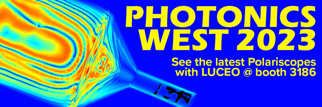
Photonics West 2023
Barnett Technical Services will be working with LUCEO in booth #4675 at Photonics West 2023, January 31 – February 2 at the Moscone Center in San Francisco.
Luceo creates highly sensitive polariscopes to analyze strain, stress direction analysis quantitative measurements in many glass and plastic applications.
Photonics West: Every year over 20,000 attendees come to hear the latest research and find the latest devices and systems that use new technologies to enable advancements in translational biophotonics, global healthcare, understanding of the brain, new lasers for manufacturing, applications of 3D technologies, photonics-based consumer products, and more.
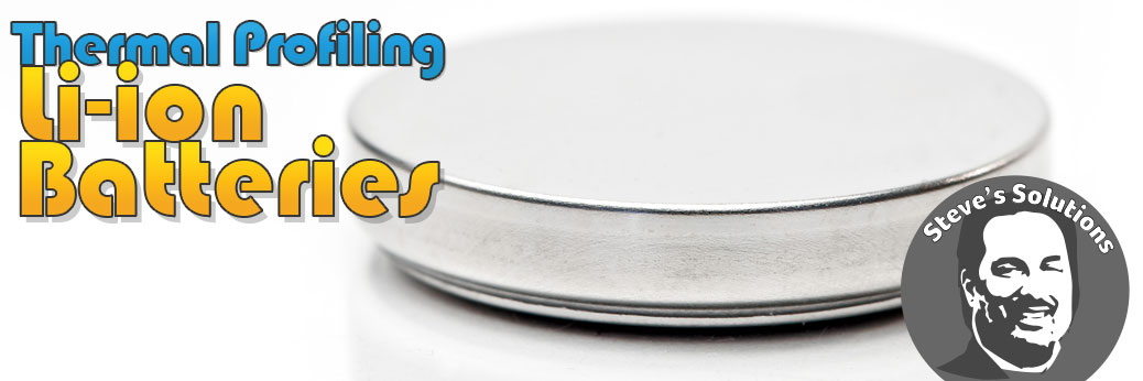
Anisotropic Thermal Conductivity and Diffusivity of Li-ion Batteries
Li-ion batteries represent many of the most critical areas of development in energy storage. The appeal of these systems arise from their higher energy densities, longer life cycles (charge and discharge), and lighter weight compared to typical battery chemistries.
To read more about our ground breaking instruments for thermal testing read the following Steve’s Solutions article.

MRS Fall 2022
We are very excited to be attending Materials Research Society Fall Meeting, November 27 – December 2, 2022, in Boston, Massachusetts. We will be at booth #509 representing a number of products:
Micro Support Micromanipulators
Manipulation of small materials.Probes available for a wide range of sample manipulations, including Isolating particles, Cutting, Milling off a surface, Nanoliquid deposition, Vacuum for material removal. Arms also be added to FTIR or Raman Microscopes.

CIQTEK
Attolight manufactures the leading cathodoluminescence (CL) microscopes and accessories on the market. These systems have been used for a range of applications, including Micro-LED characterization, Defect Visualization and Counting in Optoelectronic Materials, GaN for Power Electronics, Photovoltaic Materials, Defects in Thin Film Battery Materials and Semiconducting Diamond
About MRS
The increasingly cross-disciplinary worldwide activity in materials research manifests itself every year in the MRS Fall Meeting. Featuring over 50 symposia and attended by as many as 6,000 researchers from every corner of the globe, the annual Fall Meeting in Boston’s Hynes Convention Center and Sheraton Boston Hotel is the preeminent annual event for those in the field of materials research.
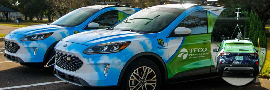
MobileGuard Gas Detection
Teco Peoples Gas hits the road in one of their new methane detection vehicles. These vehicles are going to be game changers for Peoples Gas. The Ford Escapes are outfitted with MobileGuard, a cutting-edge, laser-based analyzer that uses special software and windspeed calculations to pinpoint natural gas leaks by locating methane emissions. The sensitive sensors can detect with ultra-high precision – parts per billion, as compared with our handheld leak detection equipment which detects parts per million. That means they will detect methane emissions that you can’t smell and would otherwise go unnoticed. And, the system is smart enough to know if the methane detected is from natural gas or other sources like biogas from sewers.
ISTFA 2022: Oct 30 – Nov 3
Please join us in Pasadena California, on October 30th to November 4, for ISTFA 2022. This is always a great show and we are looking forward to meeting with friends and making new ones. Please visit us at Booth #508.
We will be at there representing a number of products:
Micro Support Micromanipulators
Microscope/micromanipulator system to easily perform sample manipulations as small as 1 micron. Probes available for a wide range of sample manipulations, including electrical probing, isolating particles, cutting, milling off a surface, micro tweezers, and vacuum for particle transfer.
Arms also be added to FTIR or Raman Microscopes.
Nanoro
The Nanoro M is a cutting edge light microscope which can break the optical diffraction limit using the Super-Resolution Microsphere Amplifying Lens (SMAL). Nanoro M benchtop super resolution microscope for imaging of semiconductor circuits with resolution under 100 μm.
About ISFA 2022, Oct 30 – Nov 3, Pasadena Convention Center
Plan today to attend ISTFA 2022! The 47rd International Symposium for Testing and Failure Analysis (ISTFA). This year’s theme is ‘ Chasing Ever Smaller and More Elusive Defects’