
Precision Micro-Wiring Modification and Repair Using Milling Pro and Tungsten Probes
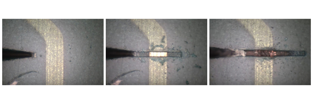
Fine wiring patterns on printed circuit boards leave very little room for error. The traces are small, closely spaced, and easily disturbed which means any modification or repair has to stay tightly controlled and precisely localized. Working at this scale generally calls for a two-stage approach: first, controlled surface removal to expose the wiring area that needs attention, and second, localized conductive-paste application to repair it. MicroSupport’s Milling Pro and tungsten probes are built for these two distinct stages of micro-wiring work.
Why Fine Wiring Requires Controlled Micromanipulation
The working area around a fine wiring trace is small, and there’s little tolerance for tool drift or imprecise movement. Successful wiring work generally depends on:
- Precise positioning: Keeping the tool or probe exactly on target throughout the operation.
- Real-time visual monitoring: Confirming progress and tool position as the work happens, not after the fact.
- Controlled material removal: Taking off only what’s needed to reach the target excessive removal or uncontrolled movement can affect surrounding wiring.
This is why fine wiring work generally calls for specialized micro-tools rather than general-purpose equipment the margin for error at this scale doesn’t allow for anything less.
Exposing Micro-Wiring with Milling Pro
Controlled Surface Scraping
Milling Pro is MicroSupport’s precision cutting and scraping tool, and one of its documented applications involves a printed circuit board wire: controlled scraping of the surface to expose the wire underneath. The demonstrated operation removes the surface material covering the wire it doesn’t cut or modify the wire itself.
Pinpoint Access to the Wiring
- Controlled depth and position: Managing cutting depth and tool position precisely removes exactly enough material to expose the target without affecting the surrounding area.
- Real-time visual monitoring: Lets the operator confirm the cut stays localized and track progress as the wire becomes exposed.
Localized Circuit Modification
Controlled scraping or cutting can also modify a specific wiring area for instance, interrupting a wiring path at a defined point, as shown in the demonstrated application. This should be read as localized cutting within that specific documented case, not a universal procedure; settings that work for one circuit and wire type won’t necessarily transfer safely to every PCB or wiring pattern.
Barnett’s Milling Pro page notes that the tool can be attached to MicroSupport micromanipulators and supports cutting with real-time visual monitoring, with listed applications including pinpoint cutting of IC packages and LCD panel encapsulation materials.
From Wiring Exposure to Localized Repair
Exposing a wiring area and repairing it are separate operations requiring different tools. Once a wiring pattern has been exposed or modified, a second documented MicroSupport application addresses what comes next: applying conductive paste to repair the pattern. This calls for a fine probe capable of precisely positioning a small amount of conductive material exactly where it’s needed. Milling Pro’s role ends at surface exposure and controlled cutting the tungsten probe handles the repair itself.
Repairing a Wiring Pattern with Conductive Paste
Precise Conductive-Paste Application
A tungsten probe is used to apply conductive paste directly to a wiring pattern or conductive feature. Controlled probe positioning is essential, since the paste needs to land precisely on a very small target area without disturbing the surrounding structure.
Example 1 Bridging a trace gap:
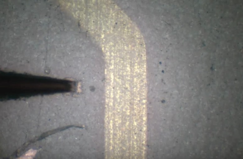
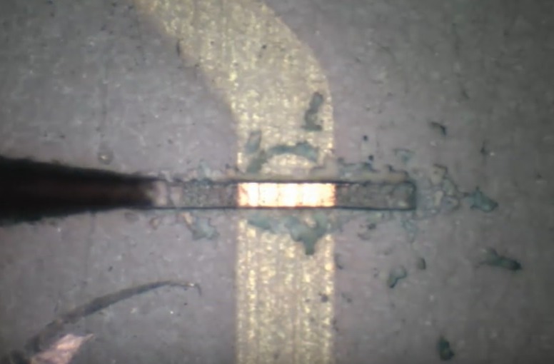
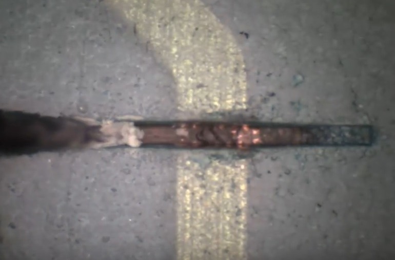
Fig 2: Pinpoint cutting of micro wiring using Milling Pro
Example 2 Connecting separated electrode pads:
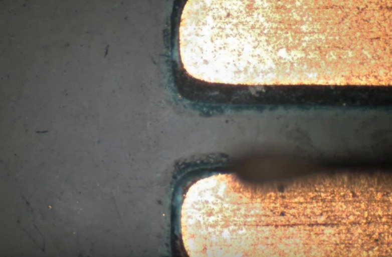
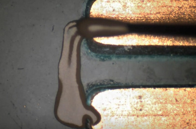
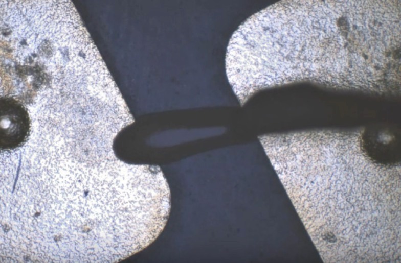
Fig3: Repair wiring with conductive paste using tungsten probe
Using a Fine Tungsten Probe
The manufacturer’s documented application for this task uses a 10 µm tungsten tip a diameter specific to the case shown, not a universal requirement. Probe selection should be based on the wiring geometry, the target area size, and the manipulation required for that particular repair.
Barnett’s Tungsten Probe page lists tip diameters ranging from 0.2 µm to 30 µm, giving a range of configurations suited to different sampling and manipulation needs.
Controlled Placement of Conductive Paste
At a high level, the process involves:
- Position the probe over the target wiring area.
- Pick up or handle the conductive paste.
- Place the paste at the required location on the wiring pattern.
- Inspect the resulting repair.
No specific paste composition, curing temperature, or electrical resistance values are documented here applying conductive paste shouldn’t be assumed to automatically restore electrical performance unless that performance has actually been verified through testing.
How the Two Applications Complement Each Other
This is the core connection between the two documented applications sequential stages of one workflow, not competing methods:
- Inspect: Identify the wiring feature and the specific area requiring attention.
- Expose or Modify: Use Milling Pro for controlled surface scraping where reaching the wiring requires removing surface material.
- Position the Repair Tool: Use a suitable micromanipulator to position the fine tungsten probe over the target area.
- Apply Conductive Paste: Use the tungsten probe to place conductive paste on the selected wiring pattern.
- Inspect and Verify: Inspect the repaired area and, where required, perform appropriate electrical testing.
Technical clarification: Milling Pro handles-controlled cutting, scraping, and surface removal. The tungsten probe handles localized handling and application of conductive paste. The micromanipulator, in both cases, provides controlled positioning of whichever tool is attached. Milling Pro does not perform conductive-paste repair the two tools are complementary, not interchangeable.
Role of Micromanipulation in Fine Wiring Work
Controlled positioning matters at every stage of this workflow. Working under suitable magnification, a micromanipulator provides the controlled movement needed to guide whichever micro-tool is attached Milling Pro during surface exposure, or a tungsten probe during paste application. The micromanipulator positions the tool; the tool performs the operation.
Selecting the Appropriate Micro-Tool
| Operation | Micro-Tool |
| Controlled surface scraping | Milling Pro |
| Localized cutting/modification | Milling Pro |
| Conductive-paste handling/application | Tungsten Probe |
| Precise tool/probe positioning | MicroSupport Micromanipulator |
Tungsten probe diameter should be selected according to the target and working geometry Barnett offers tungsten probes across a range of tip diameters, and the smallest available probe isn’t automatically the best choice; it still needs to match the wiring geometry and the operation at hand.
Applications for Precision Micro-Wiring Work
- PCB wiring inspection
- Fine wiring modification
- Microscopic circuit investigation
- Electronics failure analysis
- Localized wiring repair
- Precision conductive-paste application
- Electrical component investigation
- Research and laboratory evaluation of fine wiring structures
These represent potential application areas rather than a claim that the two documented demonstrations validate every use case listed.
Best Practices for Micro-Wiring Modification and Repair
- Inspect first: Identify the target area before beginning the operation.
- Work under magnification: Use suitable magnification throughout.
- Match the tool to the task: Select the appropriate micro-tool for the specific operation.
- Control depth and position: Manage tool position and cutting depth carefully during surface removal.
- Remove only what’s needed: Avoid taking off more material than the operation requires.
- Select the right probe diameter: Match the tungsten probe to the repair area.
- Apply paste precisely: Use conductive paste only where required.
- Avoid unnecessary contact: Keep the tool clear of surrounding structures.
- Verify the result: Inspect the repaired area, and perform electrical testing when continuity or performance needs confirming.
- Don’t assume one procedure fits all: Settings for one PCB or wiring pattern won’t necessarily apply to another.
Key Benefits of Precision Micro-Wiring Workflows
- Controlled access to fine wiring features
- Localized surface removal
- Precise tool positioning
- Fine conductive-paste application
- Reduced unnecessary disturbance of surrounding areas
- Flexible selection of micro-tools for different operations
- Support for microscopic electronics inspection and repair workflows
Modifying or repairing fine wiring patterns on a printed circuit board is a precision task with little room for error. Controlled surface scraping with Milling Pro exposes the selected wiring area, and a fine tungsten probe then handles localized conductive-paste application to repair it. The two tools play different but complementary roles, and getting a repair right depends on precise micromanipulation and real-time visual control throughout. The manufacturer applications discussed here illustrate what these techniques can accomplish in specific, documented cases not a universal repair procedure for every wiring pattern or PCB.
Barnett Technical Services provides MicroSupport micromanipulators, Milling Pro, tungsten probes, and related micro-tools for precision microsampling, electronics inspection, and microscopic sample preparation. Contact us to discuss your specific micro-wiring, inspection, or failure-analysis application.
Learn More: