Micromanipulators in FIB ex situ Lift-Out

Focused Ion Beam (FIB) Lift-Out is a sample preparation method critical for semiconductors, material sciences, and life sciences. In this technique, an ion beam slices an electron transparent membrane from a specific area of interest within a large sample. The extracted section, often just a few nanometers thick is mounted onto a TEM grid or other holder to carry out advanced structural and compositional analysis. With this procedure, researchers uncover details about the internal properties of materials, including crystal structures and defects, which are otherwise difficult to extract. Its applications range from creating intricate microstructures to preparing samples for detailed examination in transmission electron microscopy (TEM). By enabling material manipulation at this level, FIB has become indispensable for research and industrial purposes. Barnett Technical Services provides micromanipulators that perform ex situ lift-out to handle and position FIB foils with extreme accuracy.
Relevance of Micromanipulators in FIB ex situ Lift-Out
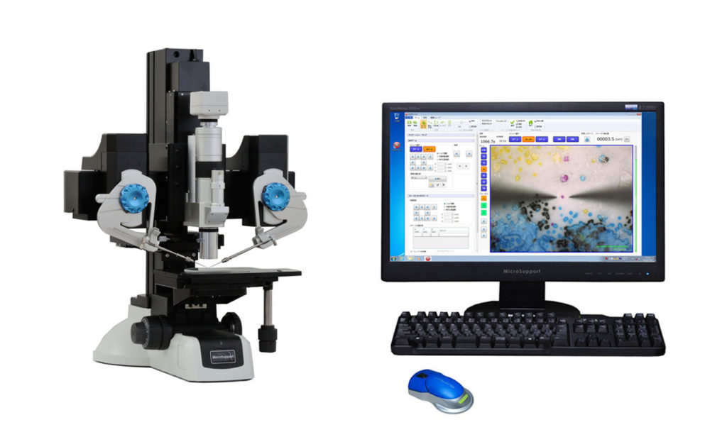
Micro Support Micromanipulators comprise of a zoom microscope, a motorized XYZ stage, and two motorized arms – designed to control movement at the microscale. They enable researchers to transfer the FIB foil to a carbon-coated copper grid or other similar sample holder for subsequent TEM analysis without causing damage, ensuring the integrity of the extracted sample for further study. With their capability to offer precise control and human error, micromanipulators help augment the accuracy and reliability of the FIB Lift-Out processes.
Benefits of Using Micromanipulators in FIB Lift-Out
Using micromanipulators in the FIB Lift-Out process has enhanced the efficiency and precision of nanoscale research. These devices streamline sample preparation, offering several notable advantages across workflow stages, as given below.
- Reduced Chamber Time For Lift-Out: Traditionally lift-out occurs in situ (inside the SEM chamber). While this method works well, it is slow and expensive for a procedure that can be handled outside the chamber (ex situ).
- High-Precision Control: Micromanipulators excel in achieving microscale precision, enabling exact positioning and alignment of samples with the ion beam. This accuracy, in turn, ensures the creation of uniform, high-quality sections critical for advanced analysis.
- Careful Handling of Delicate Samples: Materials such as semiconductor chips or biological specimens are highly stress-sensitive. Micromanipulators provide precise control, enabling gentle manipulation to avoid damage. This capability is particularly significant when dealing with ultra-thin samples or delicate structures.
- Improved Workflow Efficiency: Implementing micromanipulators helps streamline workflows, thereby reducing the time required for sample preparation. Their automation capabilities further enhance productivity, allowing for faster processing of multiple samples, and saving valuable time and resources in research and industrial applications.
- Adaptability Across Applications: Adaptable to a wide range of applications, Micromanipulators are compatible with various materials and sample types, ensuring optimal performance across industries. Its flexible, modular designs allow seamless integration with different FIB systems, making it an ideal solution for diverse industries.
Key Steps Involved in FIB Lift-Out Process Using Micromanipulators
The FIB Lift-Out process is a series of intricate steps requiring careful execution. Each stage benefits from the precision and reliability offered by micromanipulators. Following are the major steps involved in the process.
- Milling with Ion Beam: The next step involves directing the focused ion beam (FIB) to mill the sample and create a thin section. Real-time monitoring of the process helps operators refine the milling to achieve consistent thickness, while also minimizing imperfections.
- Extracting the Sample: After removal from the chamber, the micromanipulator carefully secures the milled thin section and lifts it from the rest of the bulk material. This step demands high precision to avoid damaging the fragile sample and ensuring a clean extraction. The isolated section is then placed onto a TEM grid or another suitable platform for further procedures and analysis.
- Final Adjustments: Use the micromanipulator for precise positioning and alignment of the sample to ensure it is correctly oriented for detailed investigation. Once positioned, secure the sample firmly to maintain its stability during imaging or other analytical procedures.
Applications of FIB Lift-Out in Various Industries
FIB Lift-Out has found applications in diverse fields, each benefiting from the precision and accuracy it offers.
- Semiconductors: FIB Lift-Out is critical for detecting flaws and ensuring quality assurance in microchips and other electronic parts. It enables engineers to detect defects and refine production workflows for better efficiency and reliability.
- Energy Sector: The process examines materials designed for energy applications, including storage devices like batteries and renewable energy sources such as fuel cells. It helps understands material wear and optimizing performance for longer life and efficiency.
- Materials Science: This site-specific technique is chosen to investigate the structural attributes of various materials, such as crystal lattice arrangements, grain boundaries, and phase compositions. It also supports the development of innovative materials with specific characteristics suitable for industrial needs.
- Life Sciences: The technique is imperative for preparing biological samples like cells and tissues for detailed high-resolution imaging. This supports advancements in fields such as cell biology, pharmaceutical and bioengineering as it simplifies the research related to cellular structures, protein complexes, and bioengineered materials.
- Aerospace and Automotive: The technique evaluates cutting-edge materials such as high-strength composites and advanced alloys. It assists in diagnosing material failures and enhancing material properties for operations under demanding conditions.
Why Choose Micromanipulators from for FIB Lift-Out?
We, at, Barnett Technical Services, offer a comprehensive range of micromanipulators of leading brands that are engineered to meet the demands of modern research and industrial applications. Following are the key reasons that substantiate your decision to buy this critical instrument from us.
- Proven Experience: We offer high-precision micromanipulators tailored for FIB Lift-Out from brands like Micro Support Co. Our products, including Axis Pro, Quick Pro, and Collection Pro benchtop micromanipulators are trusted by leading research institutions and industrial organizations worldwide.
- Expertise in FIB Technology: Our team’s deep understanding of FIB systems enables us to provide consulting and training services, ensuring seamless integration and optimal performance. Our experience in the chemical and materials sciences added to our capabilities to act as manufacturer’s representatives and distributors.
- Comprehensive Support Services: At Barnett, we offer extensive training, maintenance, and technical support to help our clients fully utilize the benefits of our products. Our commitment to quality and innovation is reflected in the positive feedback we consistently receive from diverse customers spanning from leading academic institutions, government laboratories, and major industrial organizations.
How Can you Optimize FIB Lift-Out with Micromanipulators
Following are several notable tips that contribute to maximizing the performance of your micromanipulators.
- Operator Training: Ensure that comprehensive training is conducted to help operators understand the operation and functionality of micromanipulators. Structured certification programs can help them gain the necessary skills to manage intricate processes effectively.
- Adopting Advanced Practices: Keep an eye on the emerging trends and developments in FIB technology and micromanipulation. Experiment with cutting-edge techniques to boost both accuracy and operational efficiency.
- Routine Maintenance: It is highly advisable to conduct periodic inspections and maintenance of micromanipulators to ensure optimal functionality and durability.
- Managing Environmental Factors: Utilize controlled settings to reduce the influence of external disturbances, such as vibrations or temperature variations, which may compromise accuracy and results.
Micromanipulators are integral to the FIB Lift-Out process, providing unmatched precision, efficiency, and reliability. Their role in enabling accurate sample preparation has made them indispensable across industries. Discover how the models we offer under the category of micromanipulators can revolutionize your research and development workflows. If you need more understanding on this cutting-edge instrument, contact the team at Barnett Technical Services today to schedule a demo, request a quote, or explore our full range of products designed for FIB Lift-Out applications.
Related Products:
Axis Pro: Benchtop micromanipulator incorporating a zoom microscope and motorized sampling arms
Quick pro: Individual micromanipulator arm that can be added to a white light microscope.
Collection Pro: Automated grain/particle sorting and collection system.
