Applications on GaN for Power Electronic

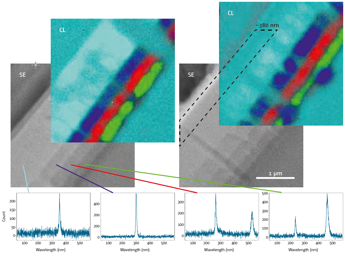
Find out how CL can investigate QD nanowires
| Field | Material | Technique |
|---|---|---|
| Fundamental and applied research | Nitride semiconductors | Hyperspectral imaging |
Abstract
Increasing emphasis on fuel economy requires electrification of the vehicle powertrain, sup- ported by the use of new power semiconductor devices dedicated to automotive applications.
Present electric vehicle systems rely exclusively on silicon-based power management, but silicon power devices are rapidly approaching maturity, and their performances are limited to address new requirements of all electric propulsion systems including high-current (200 to 600 A), high-voltage (100 to 600 V) and low-loss power semiconductor switches. Moreover, further enhancements on silicon are incremental, while the cost of advancements are increasingly uneconomical.

Next generation electric vehicles require game changing power management solutions with significantly higher efficiency and differentiating system-level advantages compared to present systems. Therefore, new electronic materials and device structures are needed. Gallium Nitride (GaN) switches are projected to have a 100× performance advantage over silicon-based devices, owing to their excellent material properties such as high electron mobility, high breakdown field, and high electron velocity. Recent progress in GaN epitaxial growth technology allows the manufacturing of GaN-on-Si wafers with high quality, low cost, and large wafer size.
Due to its compatibility with high-volume silicon fabs, the GaN-on-Si technology platform can be produced in large volume, resulting in superior performance and reduced system cost, making this technology a true game changer for automotive applications. Cathodoluminescence is one of the key techniques used in semiconductor physics. It is able to provide characterization of III-V thin film materials with a spatial resolution compatible with the size of the devices, opening a wide field of research. The Attolight CL system, thanks to its innovative configuration, provides the following advantages:
- High field of view that allow the quantification of Threading Dislocation Defect (TDD) by surface defect mapping.
- Hyperspectral mapping with acquisition speed compatible with a good spatial resolution, leading to full structure characterization on polished cross section.
- Highly stable cryostage allowing high resolution measurement at 10 K giving information of spatial distribution of defects to monitor material doping for example.
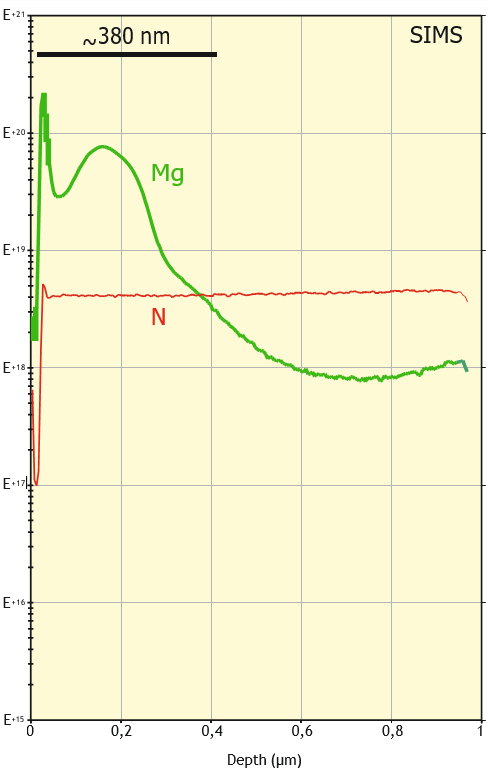
Mg profile

Source: Attolight
