Applications on Quantum Heterostructures

Find out how CL can investigate QD nanowires
| Field | Material | Technique |
|---|---|---|
| Fundamental and applied research | Arsenide semiconductors | Hyperspectral imaging |
Abstract
The second half of the 20th century has seen the emergence of semiconductor quantum structures driven by promises of far superior performances in particular regarding light emission. The dimensionality was reduced to point-like quantum dots (QDs). QDs exhibit intriguing similarities with atoms and tremendous efforts were made to assess their properties.
The growth of quantum dots embedded in filamentary crystals, known as nanowires (NWs), become relevant given the strong interaction between light and NWs. QDs in NWs are particular expected to be key elements in quantum technologies, such as quantum communications and cryptography. However, the reduced dimensionality of both QDs (ar. 5–10 nm) and NWs (ar. 100–200 nm in diameter) can strongly complicates the measurements of the QDs properties. In particular, absolute QDs position and resolution between closely lying dots is hard to assess with full-optical measurement due to diffraction limitations.


Close-up of two NWs tip. Red now represent emission from the GaAs core (820 nm) of the wire, when blue regions mark the QDs emission (670 nm). Dots at less than 500 nm can be easily resolved
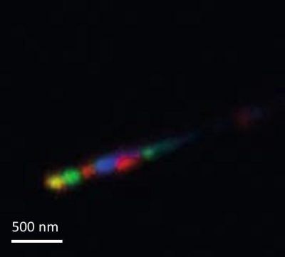
Mapping of the QDs location with respect to the emitted wavelength. Blue, green and red correspond to 3 wavelengths between 650 and 700 nm. Some dots emit are several wavelengths, resulting in composite colors (e.g. yellow)
This limit can be overcome with cathodoluminescence measurements, which makes possible the investigations on the position of QDs and their appearance depending on the properties of the host NW. For our structures, made of GaAs and AlGaAs, the Attolight CL-SEM allows us to work at cryogenic temperature, a necessary condition to observe light emission from the QDs. Furthermore, the Attolight microscope provides the following advantages compared to traditional system:
- The large numerical aperture ensures a very high signal-to-noise ratio, leading to a shorter exposure of the QDs to the electron beam and hence reducing the risk of bleaching as well as speeding up the experiment.
- Atomic Force Microscopy (AFM) can scan large areas with verygood resolution. Unfortunately, AFM measurements are usually time-consuming and can merely probe buried defects.
- The higher signal allows to use straightforwardly a spectrometer-CCD detection channel, without the need of photomultiplier tube, yielding directly fast hyper- spectral mapping. The wide emission spectral range is then captured (in our case from 650 nm to 900 nm).
- The spatial resolution permits to resolve closely lying dots as well as local features such as changes in the matrix crystal phase.
Summing up, analysis done with the Attolight system simply provide information on both the QDs and the matrix that cannot be obtained by other means without extreme effort and compromises.
Source: Attolight
