Applications on Semiconducting Diamond
Find out how CL can investigate semiconducting properties of diamond
| Field | Material | Technique |
|---|---|---|
| Fundamental and applied research | Diamond | Hyperspectral imaging |
Abstract
Due to the extraordinary properties of diamond such as extreme hardness, chemical inertness, optical transparency, high thermal conductivity in combination with electrical insulation, more and more fields of applications recognize the benefits provided by this material.
- Particularly in applications involving extremely high-power densities, high mechanical loads or severe abrasive conditions, diamond is often the only material meeting the demanding requirements. Diamond has found applications in numerous fields including:
- High-power electronics: exceptional electronic properties of diamond make it the most robust candidate for high power devices like diodes and HEMTs.
- Quantum information: Nitrogen-based vacancy centers can be used as single- photon sources.
- MEMS and bio-MEMS: diamond is a promising material for individually addressed electrode arrays.
- Optical, thermal and mechanical applications: infrared windows and lenses.
- Electro-chemical applications: electrodes and bio-chemical sensors.
- Radiation sensors: ionizing radiation detectors/dosimeters and fluorescence beam monitors.
Cathodoluminescence is one of the key techniques used in the study of semiconductor physics. Its application field goes from the analysis of defect distributions in semiconductors to the characterization of the electrical properties of such materials. All these studies have an impact on the improvement of the growing parameters and the design of high-power electronic devices.
The special features of the Attolight CL system open a new field of research:
- Full characterization of delta structures: with up to 10 nm of spatial resolution, this is one of the most powerful tools for the study of quantum wells in semiconductors.
- Complete study of carrier dynamics: charge carrier lifetimes are measured in time- resolved mode.
- Incorporation of dopants: Attolight CL system can operate at deep-UV and up to 20 K, which means optimal conditions to observe exciton spectra in diamond are met.
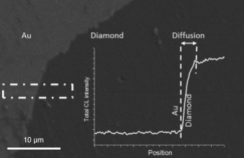
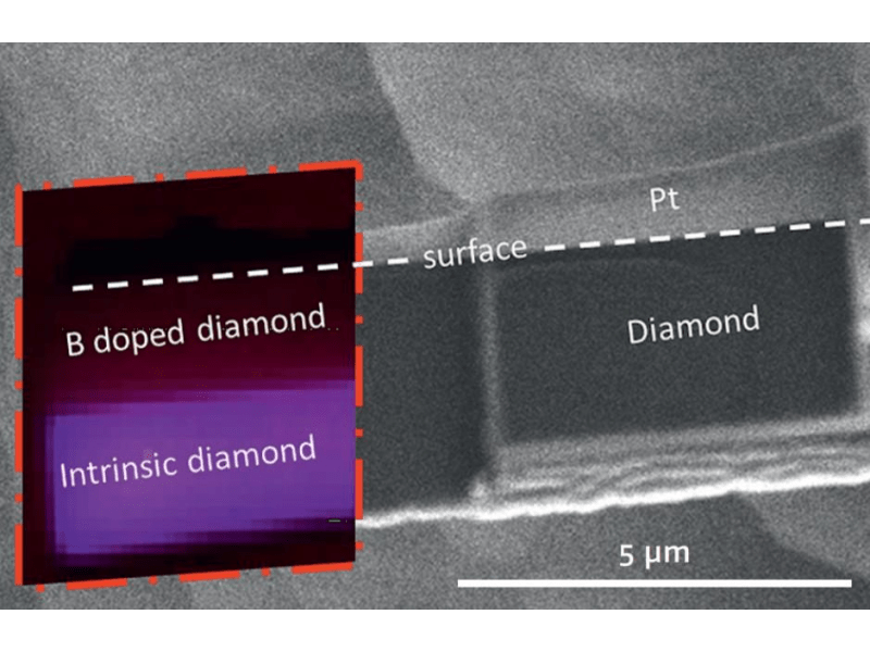
- Interface analysis: thanks to the high spatial resolution and the nano-positioning stage, it is possible to acquire interface linescans and mappings.


Source: Attolight
