AttoLight’s CHRONOS Time-Resolved Cathodoluminescence for characterizing CIGS SOLAR CELL

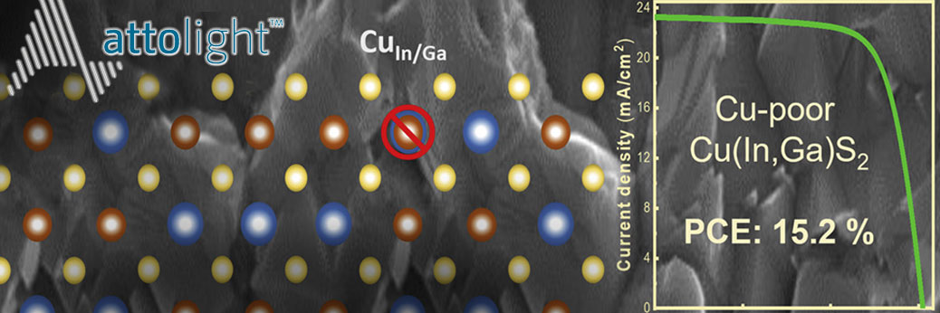
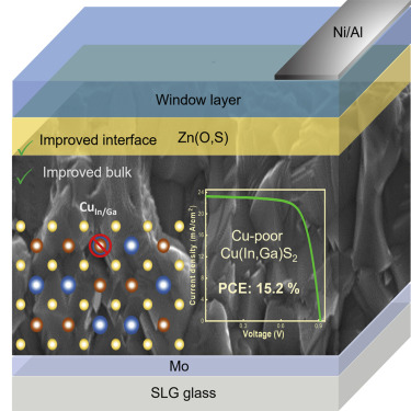
Attolight’s Chronos time-resolved cathodoluminescence tool was recently used to characterize an advanced Cu(In,Ga)S2 device that showed an efficiency of 15.2% from a H2S-free, Cd-free, and KCN-free process. significantly limited mainly due to photovoltage (Voc) losses in the bulk and at the interfaces. Here, via a combination of photoluminescence, cathodoluminescence, electrical measurements, and ab initio modeling, we address the bulk and interface losses to improve ∼1.6-eV-band-gap (Eg) Cu(In,Ga)S2. The optoelectronic quality of the absorber improves upon reducing the [Cu]/[Ga+In] (CGI) ratio, as manifested by the suppression of deep defects, higher quasi-Fermi level splitting (QFLS), improved charge-carrier lifetime, and higher Voc. We identify antisite CuIn/CuGa as a major performance-limiting deep defect by comparing the formation energies of various intrinsic defects. Interface recombination is suppressed using a Zn(O,S) buffer layer in Cu-poor devices, which leads to the activation energy of recombination equal to the Eg. We demonstrate an efficiency of 15.2% with Voc of 902 mV from a H2S-free, Cd-free, and KCN-free process.

Context & scale
Cu(In,Ga)S2 is a high-potential material for its usage in tandem solar cells; however, its power conversion efficiency has remained limited so far. High bulk recombination losses and interface losses both account for the performance limitation. In this work, we adopt a holistic approach to address both bulk and interface recombination losses. We show that bulk recombination losses can be substantially suppressed by controlling the Cu deficiency in the material. From theoretical calculations, we argue that Cu deficiency reduces the antisite defects that are probably the most detrimental defects. Additionally, we effectively passivate the interface through the usage of Zn(O,S) buffer layer, thereby minimizing the losses at the interface. This leads to a solar cell device performance of over 15% from 1.6-eV-band-gap Cu(In,Ga)S2 from a completely non-toxic process. The path to further performance improvement is discussed to increase the viability of Cu(In,Ga)S2 toward tandem application.
For More information
View Attolight Page
Visit the Attolight Website

Contact Us Online Form
Phone: 916-897-2441
Email: info@Barnett-Technical.com
