Evaluating Strain in Semiconductor Wafers Using Polariscope Stain Viewers
Semiconductor wafers are thin and circular slices of semiconductor materials used to make microelectronic devices, including integrated circuits and microchips. One of the critical aspects that must be carefully checked in semiconductor wafers is the presence of strain, which can otherwise significantly affect the performance, reliability, and lifespan of electronic devices. Strain refers to the internal stress caused by external forces or manufacturing processes – including deposition, etching, or thermal cycling – that can alter the physical properties of semiconductor wafers, leading to cracks, and other potential failures over time. So, when it comes to semiconductors, understanding, and managing strain during the manufacturing process is essential to ensure the optimal functioning of devices. This post highlights one of the most used tools for stress/strain analysis in semiconductor wafers.
Why Should You Evaluate Strain in Semiconductor Wafers?
Before getting into the details of evaluating strain in semiconductor wafers, let’s focus on the need for assessing strain in semiconductor wafers:
- Enhances Manufacturing Quality: Detecting and addressing strain during production improves the quality of semiconductor wafers, significantly minimizing the risk of defects in the final products.
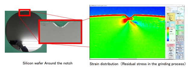
- Avoids Structural Damage: Uneven or excessive strain can result in cracks or wafer defects, potentially leading to device malfunction. Early strain detection helps avoid such structural failures.
- Improves Device Lifespan: Strain-related defects can shorten the lifespan of semiconductor devices. Regular strain evaluation guarantees reliability, contributing to the long-term durability of electronic components.
- Supports Process Optimization: Ongoing strain monitoring enables manufacturers to refine several manufacturing processes such as etching, deposition, or doping, which in turn reduces strain while also enhancing wafer yields.
- Precise Engineering: Assessing strain helps engineers design wafers with specific mechanical and electrical properties, making them apt for various specialized applications.
- Cuts Production Costs: Early identification of strain-related issues minimizes expensive repairs, reworks, or product recalls, ultimately minimizing manufacturing expenses.
- Guarantees Industry Compliance: Strain evaluation helps ensure that wafers meet the stringent quality and reliability standards mandated by various industries especially medical, military and aerospace along with regulatory bodies.
Introducing Polariscope Strain Viewers
Polariscopes are essential instruments that utilize polarized light to detect and assess stress patterns in materials such as semiconductor wafers and other transparent or semi-transparent objects. These tools are well-designed to offer a non-destructive, exact method for evaluating strain.
When the light passes through a material under stress, it undergoes a shift in its polarization. This shift is visualized as vibrant patterns or dark lines, known as birefringence, which highlight regions of stress or deformation. By studying these visual patterns, engineers can identify specific areas of strain, assess its intensity, and make informed decisions about necessary adjustments or corrections that must be implemented during production.
Benefits of Using Polariscope Strain Viewers in Semiconductor Manufacturing
Here is a list of the benefits of using Polariscope Strain Viewers in the semiconductor industry:
- Near-IR Polariscope Measurements: Use of near-IR light overcomes the limitations of UV-Vis polariscope operation which are opaque to semiconductor wafers.
- Real-Time Feedback: Detecting strain early in the manufacturing process helps prevent defects and failures in the final product, ensuring better quality. Polariscopes are designed to offer immediate strain analysis during production, enabling manufacturers to make quick refinements and optimize the process.
- Precise Detection of Strain: Polariscopes accurately visualize internal stress patterns, enabling engineers to spot even the most minor defects effortlessly, that could otherwise affect performance.
- Non-Invasive Testing: These devices offer a non-destructive way to examine semiconductor wafers, enabling strain analysis without causing damage or altering the material.
- Improved Reliability: By identifying strain-related defects, polariscopes contribute to the production of reliable semiconductor devices that last for years.
- Cost Efficiency: Strain detection at early production stage minimizes the need for expensive rework, repairs, or scrapping, leading to significant cost savings.
- Comprehensive Quality Control: As part of the quality control process, polariscopes ensure that semiconductor wafers meet strict industry standards for reliability and performance.
- User-Friendly Operation: With easy setup and straightforward usage, polariscopes allow fast and efficient strain evaluation without requiring specialized training.
Applications of Polariscope Strain Viewers
The following are a few applications of polariscope strain viewers in wafer manufacturing:
- Polariscopes are used in the quality control stage to detect and measure strain in semiconductor wafers, ensuring they meet the necessary specifications before moving to the next stage of the manufacturing process.
- During critical stages like deposition, etching, and doping, polariscopes monitor stress levels, enabling manufacturers to optimize processes and improve yield.
- By visualizing strain patterns in wafers, polariscopes provide critical data for identifying the root causes of defects and implementing corrective measures.
- Strain viewers assess stress during wafer bonding, ensuring proper alignment and reducing the risk of defects in multi-layered wafers due to strain.
- Polariscopes help assess the impact of thermal treatments like annealing, identifying any strain caused by temperature fluctuations during such processes.
- Researchers and engineers use polariscopes to study the mechanical properties of semiconductor materials, helping them understand how various materials respond to stress and strain.
- During wafer thinning and dicing, strain viewers detect stress, minimizing the risk of cracks or defects arising from mechanical processes.
- Polariscopes can identify surface imperfections such as cracks or scratches early on.
- In R&D, polariscopes are used to map strain across wafer surfaces, immensely contributing to the exploration of new materials, designs, and manufacturing techniques to enhance wafer performance.
Assessing strain in semiconductor wafers is essential for maintaining the quality, functionality, and durability of electronic devices. As mentioned earlier, tools like polariscope strain viewers deliver a precise, non-destructive method for identifying stress patterns during production, helping manufacturers avoid defects, and streamline processes. The use of a near-IR polariscope such as the Luceo LSM-9001NIR is critical for the routine evaluation of strain measurements.
Considering the critical nature of these tools’ applications, getting them from trusted sources like Barnett Technical Services, a trusted distributor of spectroscopy equipment is advisable. The company offers high-performance polariscope strain viewers, ensuring the semiconductor industry can meet its stringent strain analysis and quality assurance needs.
Related Products :
LSM-9001NIR: Near-IR system to measure strain in semiconductors.