Cathodoluminescence (CL) microscopy has transformed materials characterization, providing high-resolution imaging and spectroscopy for defect inspection, semiconductor analysis, and nanophotonics research. Attolight leads this innovation with state-of-the-art CL microscopy solutions, engineered for unmatched precision and automation. Barnett Technical Services works with Attolight to provide Multi-Spectroscopic CL SEM Platforms for advanced material analysis, CL-STEM Add-Ons to enhance electron microscopy, and Automated Wafer CL-SEM Systems for high-throughput defect inspection—ensuring superior performance, efficiency, and adaptability.
Cathodoluminescence Microscopes
Products
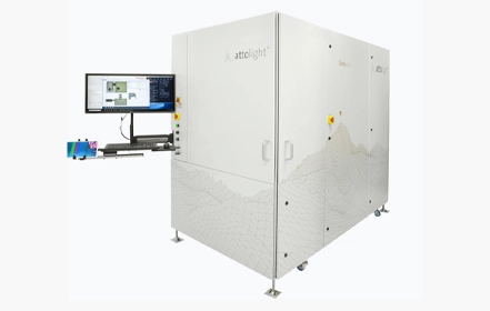
The Säntis 300 is an automated process control system for wafers up to 300 mm, offering l..
Read More..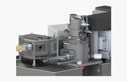
SEM – Quantitative Cathodoluminescence (qCL) Spectroscopic Analysis (Photoluminescence, ..
Read More..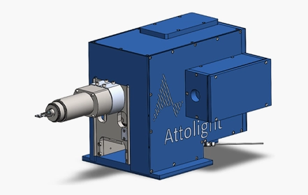
The Mönch is an advanced add-on designed for efficient light collection and injection in ..
Read More..Attolight’s Cathodoluminescence Microscopy Solutions
- Allalin: Hybridized SEM Spectroscopic Platform: The Allalin system integrates a CL microscope within a scanning electron microscope (SEM) for quantitative cathodoluminescence (qCL) imaging. Its embedded optical collection objective ensures precise, repeatable measurements. Supporting multi-spectroscopic analysis with electron and laser excitation, it also offers in-SEM electrical probing, Raman, and photoluminescence. Cryogenic sample stages (10 K – 320 K) enable temperature-dependent spectroscopy for diverse applications.
- Mönch: Light Collection & Injection for STEM: The Mönch CL STEM Add-On enhances light collection and injection in scanning transmission electron microscopy (STEM). A proprietary mirror system ensures high signal-to-noise ratio, while sub-micrometer alignment maximizes efficiency. Its dual-mode functionality enables both light collection and injection, making it ideal for advanced photonic and quantum research.
- Säntis 300: Automated Wafer CL-SEM System: The Säntis 300 is a fully automated wafer-scale CL-SEM system for semiconductor defect analysis and process control. Designed for wafers up to 300 mm with high-speed spectral and imaging acquisition. Multiple scanning modes enable process monitoring, failure analysis, and material mapping, ensuring high-precision semiconductor quality control.
What is Cathodoluminescence Microscopy?
Cathodoluminescence (CL) microscopy is an advanced imaging technique that leverages electron beam excitation to induce light emission from materials. This emitted light carries valuable information about the material’s optical and electronic properties, making CL microscopy a powerful tool for analyzing defects, structural inhomogeneities, and electronic bandgap variations at the nanoscale.Unlike conventional electron microscopy, which provides topographical and compositional insights, CL-SEM techniques offer additional spectral and temporal information, especially for compound semiconductors, enabling a deeper understanding of material properties.Key Advantages of Cathodoluminescence Microscopy
- Non-Destructive Imaging: Enables defect inspection without altering the material structure.
- High Spatial and Spectral Resolution: Provides nanoscale imaging with detailed spectral information.
- Time-Resolved Cathodoluminescence: Allows analysis of carrier dynamics and luminescence lifetime in semiconductors.
- Multi-Spectroscopic Integration: Combines SEM cathodoluminescence with Raman, photoluminescence, and electrical probing for comprehensive characterization.
- Automated Defect Inspection: Ideal for large-scale semiconductor wafer analysis with high reproducibility and throughput.
Applications of Cathodoluminescence Microscopy
- Semiconductor Industry: Defect inspection, dopant distribution, and process control.
- Nanophotonics: Analysis of optical properties in photonic crystals and plasmonic devices.
- Geoscience & Mineralogy: Identification of mineral composition and growth history.
- Materials Science: Investigation of strain, defects, and phase transitions in advanced materials.