Technical
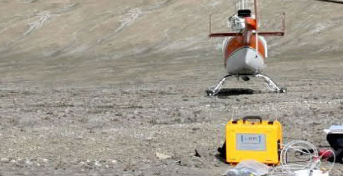
Soil Flux Analysis
Greenhouse gases (GHGs) such as CO2, CH4 or N2O released from various soils in the…
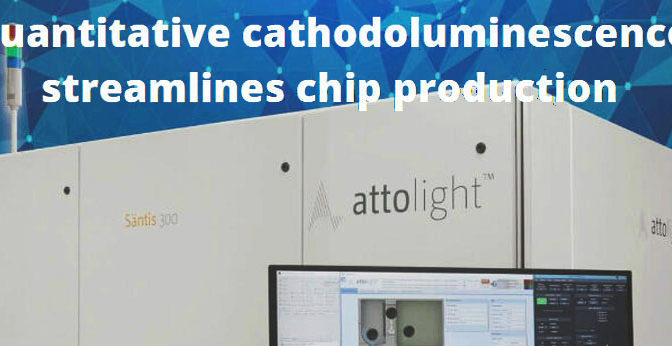
Quantitative cathodoluminescence streamlines chip production
Cathodoluminescence offers a quick, non-invasive approach to determining alloy compositions, exposing defects and uncovering surface…
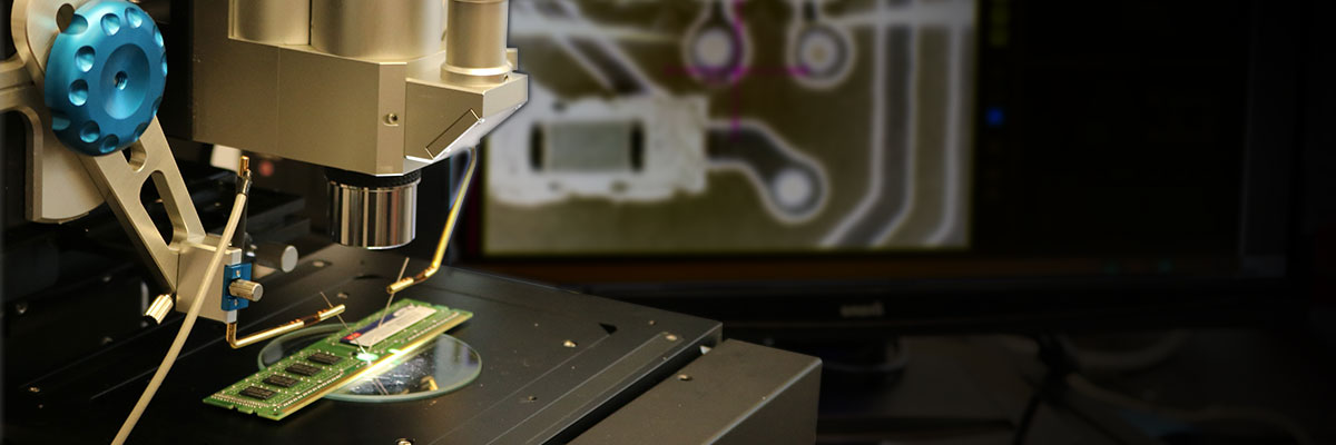
Award for work using micro manipulator
Geophysical Laboratory's Zachary Geballe Receives Seventh Postdoctoral innovation and Excellence Award The Geophysical Laboratory’s Postdoctoral…
Micro Support Users Meeting Wrap Up
We had the first North American Micro Support Users Meeting on Thursday, May 10th at…
Micro Support Users Meeting – Wrap up
We had the first North American Micro Support Users Meeting on Thursday, May 10th at…
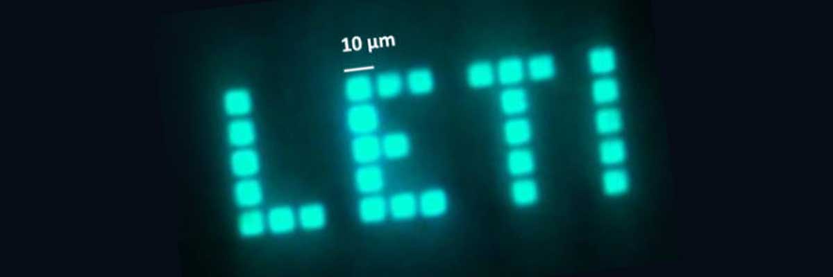
Attolight CL for Micro-LED Characterization
Some great display technology here. Attolight's cathodoluminescence products provide capabilities needed for assessing the quality…
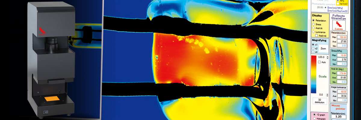
Luceo Fullauto StrainEye LSM-9000S
Luceo Fullauto StrainEye LSM-9000s Fullauto StrainEye LSM-9000S is a fully automatic 2D-measuring device which measures…
Micro Support Users Meeting – May 10, 2018
This workshop will bring together scientists from throughout the U.S. to share best practices in their…